On-chip nanophotonic topological rainbow
来源: 作者: 发布时间:2022-10-13
Prof. Cuicui Lu et al., from the School of Physics, Beijing Institute of Technology, proposed the method of constructing multi-frequency topological states by adopting synthetic dimensions and realized the on-chip topological rainbow nanophotonic device. This work was published in Nature Communications.
Nanophotonic devices, which take photons as information carriers, have important applications in optical communication, optical information processing, optical computing, and other fields. The smaller of the device, the higher of the integration density; however, there will be larger influences on device performance by errors at the nanoscale. Topological photonic states protected by topology have the advantages of robustness and anti-interference compared with traditional photonic states. Therefore, topological photonic states provide a new platform for the realization of nanophotonic devices. As a freedom degree of photons, frequency is a basic information carrier. Therefore, constructing multi-frequency topological photonic states to realize broad operation band provides a method to realize robust nanophotonic devices for big data information processing.
Prof. Cuicui Lu et al. proposed to use the synthetic dimension method based on lattice translation and rotation to construct on-chip integrated multi-frequency topological nanophotonic devices. This work opened up the research direction of on-chip topological rainbow nanophotonic related devices. Invited by the editor-in-chief of Applied Physics Letters, the perspective article "Perspective on the topological Rainbow" was published (Sayed Elshahat, Chenyang Wang, Hongyu Zhang, Cuicui Lu,* Appl. Phys. Lett. 119, 230505, 2021). Because the device is protected by topology, as long as the photonic crystal bandgap is not closed, the performance of such topological rainbow devices is robust when the device experiences structure scaling, random error, material defect, or impurity interference.

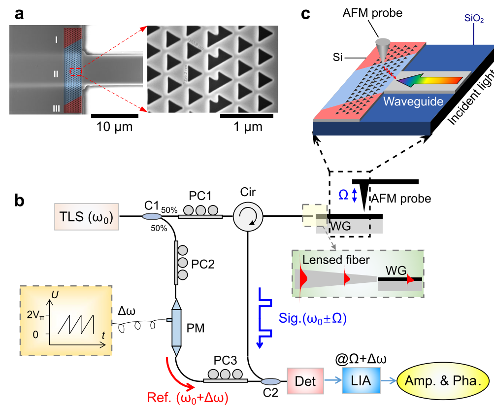
Fig. 1 (a) SEM images of the sample. (b) Experimental setup. (c) Amplified schematic diagram of the electric field detection.
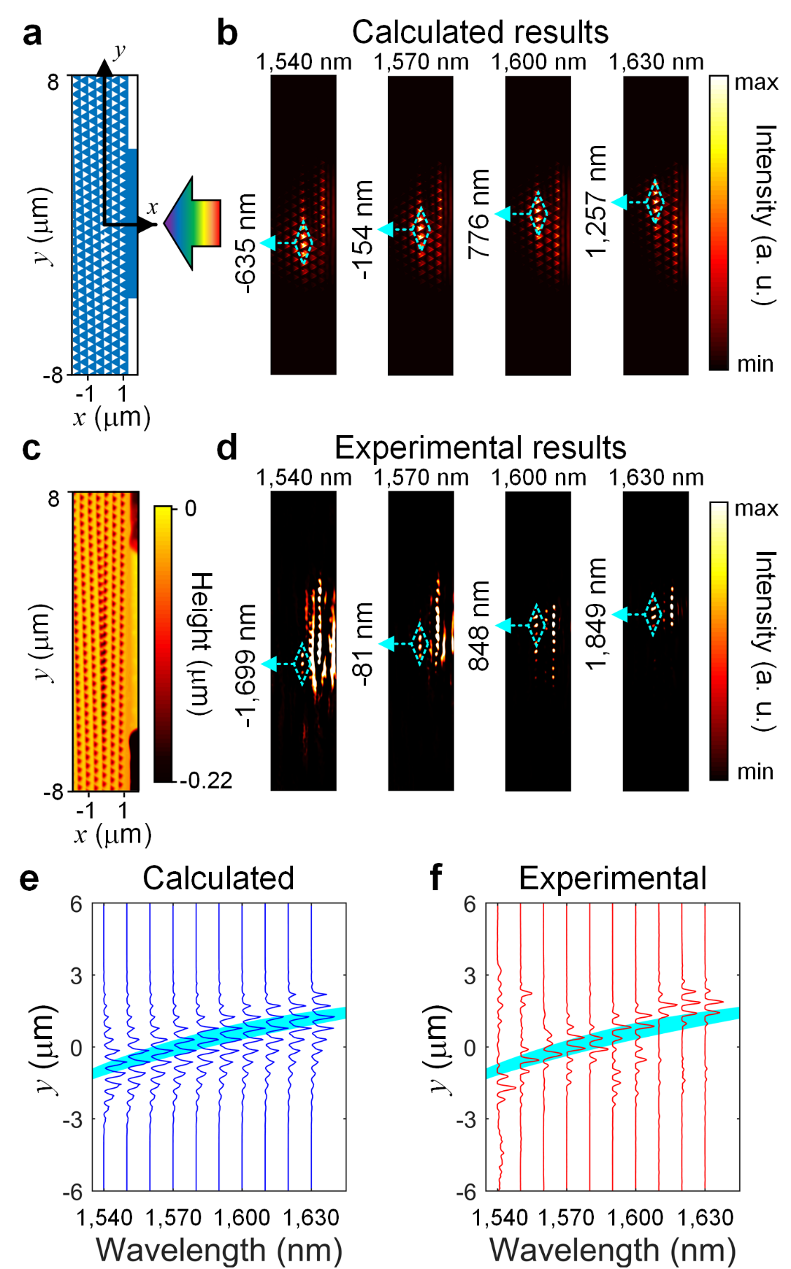
Through the homemade near-field optical microscopy system by Prof. Wei Ding, the electric field of the topological rainbow nanophotonic device is observed directly. The electric field distribution of every photonic crystal lattice is clearly visible. The maximum electric field intensity of topological states with different frequencies appears at different positions. The homemade scattering near-field optical characterization technology has obvious advantages. First, the morphology of the sample and the optical signal can be measured simultaneously. So, it can directly provide the electric field amplitude signal at different positions of the photonic crystal. Second, the nonporous Atomic Force Microscope (AFM) probe is able to penetrate deep into a single photonic crystal air hole with an extremely high resolution because its tip size is only 20 nm. In addition, the waveguide end-coupling excitation method is used to improve the excitation efficiency. The optical fiber is used to collect the fiber signal on the sample surface, which has the advantages of high collection efficiency and low background noise. It is also the first topological rainbow photonic device integrated into the nanoscale, which establishes a bridge between the frontier research of topological photonics and the mature technology of silicon-based photonics.

Fig. 2 (a) The top view of the FDTD model. (b) The light intensity distributions (|E|2) of the calculated results for different wavelengths. (c) The topographic image of the sample. (d) The light intensity distributions of experimental results for different wavelengths.
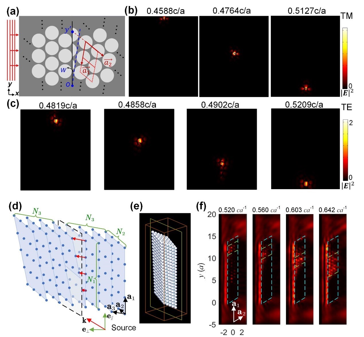
It is also found that the on-chip topological rainbow can also be achieved through photonic crystal lattice rotation. The topological states have a more compact electric field distribution, and the electric field distribution of the topological rainbow without overlap can also be achieved by adjusting the structure or material parameters. In addition, the topological rainbow phenomenon exists stably when the two-dimensional synthetic photonic crystal on the chip is extended to the high-dimensional spatial photonic crystal. The topological states with different frequencies are separated and trapped in different positions in space. The research on the topological rainbow provides a reliable method to solve the robustness of on-chip integrated router devices, wavelength demultiplexer devices, photonic caching devices, slow optical devices, and other nanophotonic devices.

Fig. 3 (a-c) Topological rainbow trapping effect based on lattice rotation. (d-f) Topological rainbow trapping in space.
Prof. Cuicui Lu is the first and co-corresponding author, Prof. Xiaoyong Hu and Prof. Wei Ding are the co-corresponding authors, Dr. Yizhi Sun and Dr. Chenyang Wang are the co-first authors. The authors gratefully thank Prof. Ling Lu for his kind help to use related optical measurement equipment in Chinese Academy of Sciences and thank Prof. Z. Q. Zhang for the helpful discussions. This work was mainly supported by the National Natural Science Foundation of China, National Key Research and Development Program of China, Guangdong Basic and Applied Basic Research Foundation, the Fundamental Research Funds for the Central Universities, and Hong Kong Research Grants Council and AoE/P-02/12, and the Croucher Foundation The authors also acknowledge the Analysis & Testing Center of Beijing Institute of Technology for the use of FIB.
Paper information:
Cuicui Lu,* Yi-Zhi Sun, Chenyang Wang, Hongyu Zhang, Wen Zhao, Xiaoyong Hu,* Meng Xiao, Wei Ding,* Yong-Chun Liu, C. T. Chan, "On-chip nanophotonic topological rainbow", Nature Communications, 13, 2586 (2022).
The paper link: https://www.nature.com/articles/s41467-022-30276-w


